-
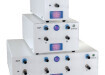
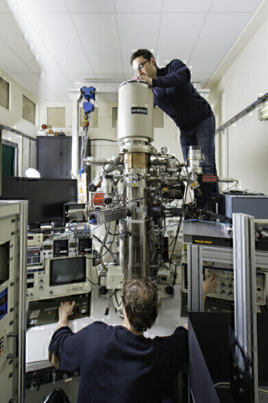 CEMES researchers handling the prototype of the ultrafast coherent ultrafast TEM microscope.
News & Views
Joint International Laboratory to Develop Ultrafast TEM
Aug 16 2018
A new electron microscope that can scan the properties of matter on very small scales of time and space is being developed by French researchers and Japanese engineers following the creation of a joint laboratory this year. The partnership between the Centre d'élaboration de matériaux et d'études structurales (CEMES) of the CNRS and Hitachi High Technologies Corporation (HHT) has been developing since 2009, when HHT engineers modified one of their products and developed a novel electron optical platform. At the same time, a CEMES team1 developed a one-of-a-kind coherent2 source of ultrafast electrons that they successfully tested on a previous generation HHT microscope, making this prototype the first ultrafast coherent TEM.
With HHT engineers seeking to collaborate on this new technology and CEMES researchers to continue this research on a more modern microscope, the two partners subsequently decided to establish the joint laboratory which was confirmed by the signing of an agreement on July 2 at the French Embassy in Tokyo.
The collaboration will revolve around the transfer of the coherent electron source to a cutting-edge model loaned by HHT in connection with this new partnership.
The ultrafast TEM project, which made possible the development of the first prototype of this technology, combines TEM and ultrafast lasers. TEM offers excellent spatial resolution as well as low temporal resolution: in short, the TEM enables the study of physical phenomena on the atomic scale at a given instant, rather than following their evolution over time. The CEMES instrument frees itself of this limitation through a new electron gun that can generate ultrashort pulses thanks to its coupling with an ultrafast laser. Using a coherent pulsed source like this one enables the study of physical phenomena—such as the dynamics of electrical or magnetic fields, or stress within nanomaterials—over very-short durations, all while observing on the sub-nanometric3 scale.
The formation of the joint laboratory between CEMES and HHT will help to achieve the goals of developing ultrafast TEM technology integrated in a modern TEM with new forms of imagery that could offer research teams a much more accurate instrument to successfully complete these unique types of studies.
1 Supported financially by the CNRS physics institute and the ANR
2 With a coherent source, the electron beam for visualizing objects in the microscope carries the same amount of energy and travels on the same trajectory. This excellent consistency is needed to image structures and fields.
3 One nanometer (nm) equals 0.000000001 = 10 -9 meters


Digital Edition
Lab Asia 31.2 April 2024
April 2024
In This Edition Chromatography Articles - Approaches to troubleshooting an SPE method for the analysis of oligonucleotides (pt i) - High-precision liquid flow processes demand full fluidic c...
View all digital editions


Events
Apr 28 2024 Montreal, Quebec, Canada
May 05 2024 Seville, Spain
InformEx Zone at CPhl North America
May 07 2024 Pennsylvania, PA, USA
May 14 2024 Oklahoma City, OK, USA
May 15 2024 Birmingham, UK